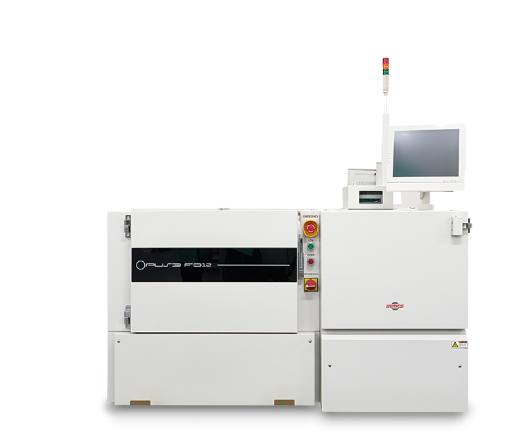
OPUS3 FD12
OPUS3 FD12 is optimized prober that handles both Standard and Frame wafer.
The Standard and Frame wafer can be converted by conversion kit conveniently.
Alignment algorithm is advanced technology for various and special wafers.
It makes high accuracy for consistent contact / probing and fast index time for higher throughput.
Key features Overview
- Universal wafer handling kit for Standard wafer & Frame wafer such as Thin, Sawn, Reconstructed and Mems wafer
- Alignment algorithm to precisely measure die offset for film sagging
- Support for all types of maps
- Retest probing with Standard and Frame wafer
- Easy & Fast conversion of Hardware and Software
- Compact system size for space efficiency
- Intelligent pin alignment algorithm
- Accurate and various shapes of probe mark inspection
- Compatible with all type of tester
- Compatible with Pogo, DD type Card changer
- Support for OCR and Barcode read
- Optimized ESD technology
Specification Overview
| Name | OPUS3 FD12 |
| Wafer Size | 280ø & 400ø Frame ring for 6, 8 & 12 inch wafer |
| 8 & 12 inch standard wafer | |
| Dimension | 1575(W) x 1939(D) x 1080(H) |
| X, Y Probing Area | X : ±180mm |
| Y : ±175mm | |
| Needle Force | 450kgf (Z Probing Force) |
| XY Accuracy | X : +1.5㎛ |
| Y : ±1.5㎛ | |
| Tri-Temp | Framed Wafer : Room temperature |
| Standard Wafer : COLD: -40℃ / -55℃; HOT: 150℃ / 200℃ | |
| AMBIENT CONTROL (25℃) |

